English
 Spanish
 French
 German
 Italian
 Chinese (Simplified)
 Japanese
 Korean
 Arabic
 Portuguese

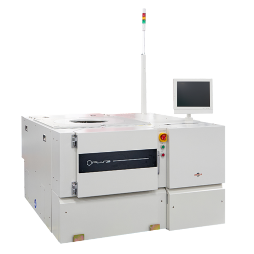
OPUS3 Prober handling SEMI standard wafers
Product Details:
- Insulation Material Industrial-Grade Insulating Plastics
- Surface Finish Powder Coated, Anodized Surfaces
- Shape Rectangular Base, Circular Chuck
- Operating Temperature 15C to 35C
- Connector Type SMEMA, USB, RS232
- Mounting Type Floor Standing
- IP Rating IP20
- Click to View more
X
OPUS3 Prober handling SEMI standard wafers Price And Quantity
- 1 Set
- XYZ Fully Programmable
- Class 1000 (ISO 6) Standards
- USB, Ethernet, RS232
- Vacuum Chuck with Automatic Alignment
- 100 m to 1000 m
- Up to 25 wafers per batch
- Precision Stepper Motors
- 150 mm (6), 200 mm (8), 300 mm (12) SEMI standard
- <5 m
- Emergency Stop, Interlocked Doors
- SEMI, CE
- Optical Alignment
- Touch Screen HMI & Remote PC Interface
OPUS3 Prober handling SEMI standard wafers Product Specifications
- Industrial-Grade Insulating Plastics
- Handles 6, 8, 12 SEMI Standard Wafers
- 220 V AC 10%
- Aluminum Alloy, Steel, High-grade Plastics
- 220 VAC
- White & Grey
- 15C to 35C
- Single Phase
- 50/60 Hz
- Powder Coated, Anodized Surfaces
- Automatic Wafer Prober
- Rectangular Base, Circular Chuck
- 20% - 80% (Non-Condensing)
- Integrated Thermal Cutoff
- Approx. 500 W
- SEMI Standard ESD Protection
- >0.9
- SMEMA, USB, RS232
- Floor Standing
- IP20
- 950 mm x 800 mm x 1450 mm
- Semiconductor Wafer Testing and Handling
- Electrical, Data Output
- Programmable, High Precision, Automated Handler, SEMI-Compliant
- >95%
- Standard Electrical Connectors, USB/Data Ports
- Approx. 150 kg
- XYZ Fully Programmable
- Class 1000 (ISO 6) Standards
- USB, Ethernet, RS232
- Vacuum Chuck with Automatic Alignment
- 100 m to 1000 m
- Up to 25 wafers per batch
- Precision Stepper Motors
- 150 mm (6), 200 mm (8), 300 mm (12) SEMI standard
- <5 m
- Emergency Stop, Interlocked Doors
- SEMI, CE
- Optical Alignment
- Touch Screen HMI & Remote PC Interface
Product Description
Product Description
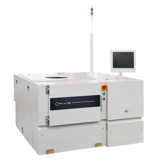
Opus3 is the only prober in the market which handles 6",8" and 12" SEMI Standard wafer, without having any change kit. It is compact, with high accuracy for consistent contact/ probing and fast index time for higher throughput. It is possible to load universal probe card.
Product Features
Compact size for space efficiency
Universal probe card changer
Reliable temperature control
Stiff and strong Z structure
Map shift prevention
Real-time recipe validation
Intelligent pin alignment algorithm
Smart probing route algorithm
Flat loader for smartest foot print
Compatible with all type of tester
Universal probe card changer
Reliable temperature control
Stiff and strong Z structure
Map shift prevention
Real-time recipe validation
Intelligent pin alignment algorithm
Smart probing route algorithm
Flat loader for smartest foot print
Compatible with all type of tester
Product Specification
Our Company

Semics Inc. is a semiconductor test equipment provider that produces fully automatic wafer probe systems (6",8", and 12") integrated with its advanced technology.
"SIMPLICITY & PERFECTION"
MAKING A DIFFERENCE BY TAILORING SOLUTIONS TO CUSTOMER NEEDS.
Since our establishment in 2000, "Simplicity & Perfection has been heart of our corporate values. It drives us to continuously grow sustainably and stay ahead with outstanding performances even under difficult market situations and changes.
"INNOVATION IN TECHNOLOGY"
OUR ULTIMATE DRIVING FORCE FOR INDUSTRY RECOGNITION
We take our mission seriously to nurture the corporate value and ensure each and every employee understands and joins our vision: Number ONE Leader in probing market by 2025.
Seamless Wafer Compatibility
The OPUS3 Prober efficiently handles SEMI standard wafers in 150 mm, 200 mm, and 300 mm diameters, with thickness ranges from 100 m to 1000 m. This broad compatibility ensures adaptability across various semiconductor production lines and research environments. Whether producing or testing new wafer technologies, the automatic alignment and programmable handling features contribute to consistent and repeatable results.
Advanced Precision and Automation
Engineered for high-performance semiconductor operations, the OPUS3 Prober showcases programmable XYZ motion, sub-5 m positioning accuracy, and optical alignment for superior precision. The integration of stepper motors and smart control systems enables automated wafer loading and unloading, maximizing throughput and minimizing manual intervention. This advanced precision is matched by robust safety and ESD protection, safeguarding both operators and delicate wafer structures.
FAQ's of OPUS3 Prober handling SEMI standard wafers:
Q: How does the OPUS3 Prober achieve high positioning accuracy during wafer alignment?
A: The OPUS3 Prober utilizes a precision vacuum chuck with automatic optical alignment and programmable XYZ motion, assisted by stepper motors. This system ensures that wafers are aligned and positioned with an accuracy of less than 5 m, crucial for semiconductor testing and processing.Q: What types and sizes of wafers can the OPUS3 Prober handle?
A: This prober is compatible with SEMI standard wafers in diameters of 150 mm (6"), 200 mm (8"), and 300 mm (12") and thicknesses between 100 m and 1000 m, accommodating a wide range of wafer specifications used in the industry.Q: When should I use the OPUS3 Prober's automated loader feature?
A: The automated loader is ideal for high-throughput environments or batch processing, as it enables handling up to 25 wafers per batch efficiently. It reduces operator workload and the risk of contamination, making it perfect for semiconductor fabs and testing labs seeking operational efficiency.Q: Where is the OPUS3 Prober best utilized?
A: The OPUS3 Prober is designed for cleanroom environments up to Class 1000 (ISO 6) and is commonly used in semiconductor manufacturing, quality control laboratories, and research facilities that require precise wafer alignment and handling.Q: What are the main safety and compliance features of the OPUS3 Prober?
A: The system is equipped with emergency stop functions, interlocked doors, integrated thermal cutoff for overheating protection, and ESD safeguards. It complies with SEMI and CE standards, ensuring operational safety and international compatibility.Q: How do I interface or control the OPUS3 Prober?
A: Operators can control the prober using a touch screen HMI or remotely through a PC interface. Data interfaces such as USB, Ethernet, and RS232 allow for versatile integration with existing systems and enable data output for process monitoring and analysis.Q: What benefits does the OPUS3 Prober offer to semiconductor manufacturers and researchers?
A: Key benefits include high precision, full automation, SEMI-compliance, programmable control, efficient handling of multiple wafer sizes, robust safety features, and reduced process variability-all contributing to higher throughput and consistent quality in wafer handling and testing.Tell us about your requirement

Price:
Quantity
Select Unit
- 50
- 100
- 200
- 250
- 500
- 1000+
Additional detail
Mobile number
Email

![[POREST N] Leaf](https://cpimg.tistatic.com/09584125/b/4/-POREST-N-Leaf.png?tr=w300)
![[UJIN LED] LED MARINE LANTERN](https://cpimg.tistatic.com/10079956/b/4/-UJIN-LED-LED-MARINE-LANTERN.png?tr=w300)